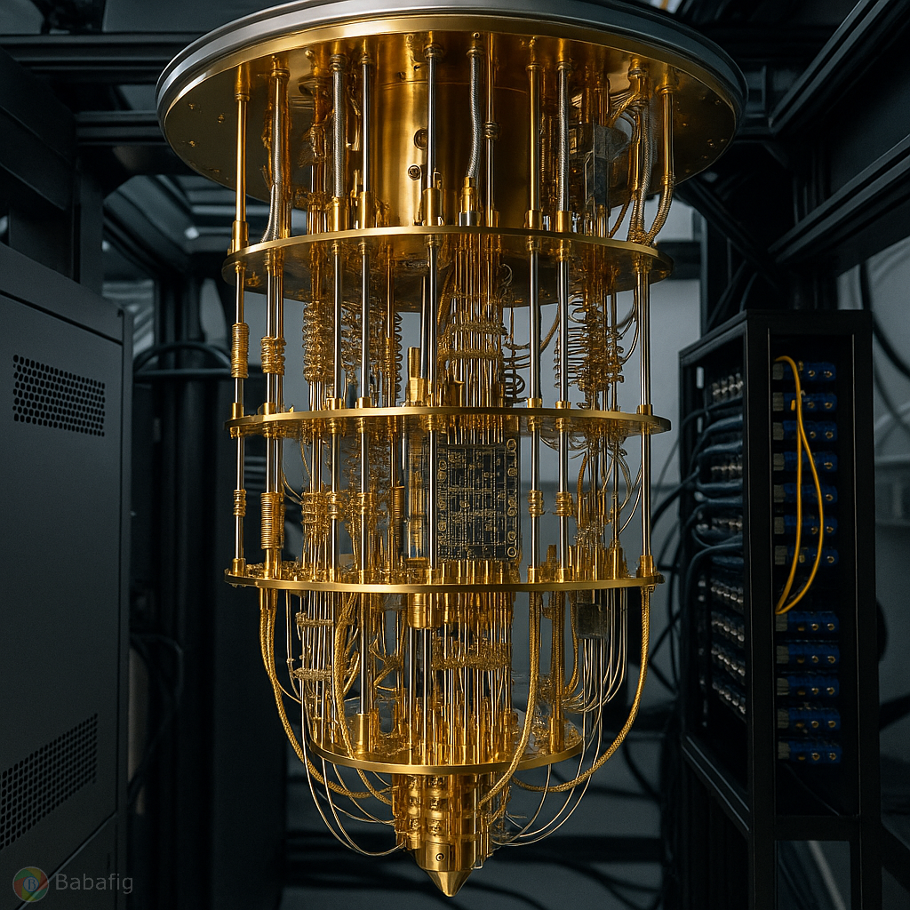
Voici une vue d’ensemble de la technologie des ordinateurs quantiques tels qu’ils existent aujourd’hui, avec les grandes familles de qubits, ce qu’elles permettent et leurs défis.
1) Le principe de base
- Un qubit est l’unité fondamentale d’information quantique. Contrairement à un bit classique (0 ou 1), un qubit peut être en superposition (0 et 1 en même temps) et peut être intriqué avec d’autres qubits.
- Les ordinateurs quantiques exécutent des portes quantiques (analogues à des portes logiques classiques mais agissant sur les états quantiques) et mesurent les résultats pour obtenir une réponse. Leur efficacité dépend fortement de la fidélité des portes et de la cohérence des qubits.
- Deux grands enjeux: l’erreur (bruit) et la stabilité des états quantiques; pour être réellement utiles, il faut soit des qubits très fiables, soit des techniques de correction d’erreur quantique qui utilisent beaucoup de qubits physiques pour protéger un qubit logique.
2) Les technologies dominantes des qubits aujourd’hui
- Qubits supraconducteurs (transmons)
- Comment ça marche: des circuits Josephson dans des puces cryogéniques, manipulés par impulsions micro-ondes et couplages via des cavités ou des liaisons.
- Avantages: contrôle rapide des portes (gates de l’ordre de quelques dizaines de nanosecondes), intégration sur une même puce et possibilité d’assembler des centaines de qubits.
- Défis: la cohérence est limitée (cohérence typique de dizaines à quelques centaines de microsecondes), et le bruit de contrôle/crosstalk peut devenir important à grande échelle; nécessite des refroidisseurs à très basse température (quelques millikelvins).
- État actuel: utilisés par des acteurs majeurs (IBM, Google, Rigetti et autres) avec des processeurs comportant des dizaines à des centaines de qubits; taux de porte à deux qubits autour de 99% et plus pour les meilleurs dispositifs, mais cela varie selon le fabricant et la puce.
- Ions piégés (trapped ions)
- Comment ça marche: ions chargés piégés (par exemple Ca+, Sr+, Yb+) manipulés par des lasers; les états hyperfins servent de qubits; les portes entanglées utilisent des interactions laser (Mølmer–Sørensen, etc.).
- Avantages: coherence très longue (sécondes à minutes), très hauts niveaux de fidélité pour les portes simples et deux-qubits (souvent >99.9% dans certains bancs d’essai), et connectivité quasi illimitée (tout qubit peut être couplé à tous les autres dans le même piège).
- Défis: vitesse des portes plus lente que les qubits supraconducteurs (gates typiquement dans les microsecondes à dizaines de microsecondes), et complexité des systèmes laser et du refroidissement qui peut limiter la scalabilité pratique.
- État actuel: utilisé par Quantinuum/Honeywell, IonQ et d’autres, avec des familles de processeurs allant de dizaines à quelques dizaines de qubits, avec des taux de fidélité très élevés.
- QuBits à base d’atomes neutres (arrays dans des optical tweezers)
- Comment ça marche: atomes neutres piégés par des réseaux de fokes optiques, entremêlés par des états Rydberg qui permettent des portes deux-qubits rapides et contrôlées par laser.
- Avantages: potentialité de très grande échelle (centaines à milliers de qubits) avec des assemblages en 1D/2D; bonne fidélité et excellente scalabilité spatiale; fonctionnement à température ambiante en apparence mais nécessitant des systèmes laser et des pièges élaborés.
- Défis: dépendance à des lasers ultra-stables et à une ingénierie optique complexe; les portes peuvent être sensibles à la déphasing et à la stabilité des faisceaux.
- État actuel: prototypes et démonstrations avec des dizaines à centaines de qubits; les efforts se poursuivent pour atteindre des architectures modulaires et robustes.
- Photons et informatique quantique photoniques
- Comment ça marche: qubits encodés dans des états de lumière (polarisation, chemin, etc.), portes réalisées par des interféromètres et des sources/ détecteurs proches du contenu quantique.
- Avantages: fonctionnement à température ambiante (ou avec des composants optiques sur puce), faible dégradation du quantum état pendant le transport (fidélités élevées sur certains systèmes), excellente coopération inter-logiciels et inter-réseaux (réseaux quantiques).
- Défis: les portes deterministes sont difficiles à réaliser; beaucoup de démonstrations reposent sur des portes probabilistes et des techniques de post-traitement; intégration et détection haut rendement exigent des composants très performants.
- État actuel: utile surtout pour des démonstrations et des expériences en téléportation, abonnement et communication quantique; des progrès importants sur les puces photoniques et les interconnecteurs.
- Qubits topologiques (recherche)
- Idée: qubits protégés par des états topologiques (par ex. quasi-particules de type Majorana) qui pourraient offrir une tolérance intrinsèque à l’erreur.
- Avantages potentiels: grand pas vers des ordinateurs quantiques tolérants aux fautes avec un overhead d’erreur beaucoup plus faible.
- Défis: reste en grande partie expérimental et non commercialisée à grande échelle aujourd’hui; barrière technique majeure pour démontrer des qubits topologiques robustes dans des systèmes pratiques.
- État actuel: très prometteuse en théorie et dans des prototypes limités, mais pas encore un pilier industriel.
3) Comment on construit et exploite un ordinateur quantique aujourd’hui
- Architecture matérielle: autour du « cœur » (la puce de qubits) s’ajoutent des outils de contrôle (électronique RF/microwave, lasers selon les technologies), des systèmes de refroidissement (pour les qubits supraconducteurs), des interconnexions et des interfaces logiciel-matériel.
- Bruit et correction d’erreur: les ordinateurs quantiques actuels opèrent largement dans l’ère NISQ (Noisy Intermediate-Scale Quantum). Cela veut dire: des qubits pas parfaits, des fautes qui s’accumulent, et un recours important à des algorithmes hybrides (quantique + classique) comme VQE (variational quantum eigensolver) et QAOA (quantum approximate optimization algorithm).
- Correction d’erreur quantique: conceptuellement nécessaire pour des calculs à grande échelle et fiables. Elle nécessite beaucoup de qubits physiques pour protéger chaque qubit logique et met en avant des codes comme le code de surface. Le seuil de fault tolerance est d’environ 0,5–1% d’erreur par porte dans beaucoup de modèles; atteindre une efficacité pratique demande des quantités massives de qubits et des améliorations de fidélité.
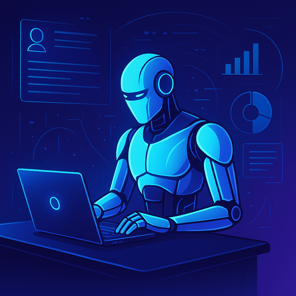
- Logiciel et toolchains: frameworks comme Qiskit (IBM), Cirq (Google), PyQuil (Rigetti), Braket (AWS) et tket permettent de concevoir des circuits quantiques, de les compiler sur le matériel spécifique et d’exécuter les expériences. Le développement logiciel inclut également des méthodes d’atténuation d’erreurs et des approches de compilation optimisée.
4) Ce que l’on peut faire aujourd’hui et ce qui change peu
- Applications potentielles à court terme: simulation de systèmes quantiques (chimie et matériaux), optimisation de réseaux/itineraries, certains problèmes d’algèbre linéaire et d’algorithmes d’optimisation pour lesquels les promesses sont encore en phase expérimentale.
- Avantages concrets restent limités: pour des tâches pratiques à grande échelle, il faut encore des centaines voire des milliers de qubits fiables grâce à la correction d’erreur; on voit surtout des avancées en démonstrations et en prototypage, avec des résultats prometteurs mais pas encore « produits commerciaux largement disponibles » dans la plupart des domaines.
- Tendances futures: progression accélérée dans le nombre de qubits, amélioration des fidelités, architectures modulaires et interopérables (par ex. réseaux de qubits interconnectés), et avancées en correction d’erreur pour réduire l’overhead.
5) Pour qui et comment s’y préparent les entreprises et les chercheurs
- Entreprises privées: IBM, Google, Rigetti (qubits supraconducteurs), IonQ et Quantinuum (trapped ions), des startups dans les domaines des atomes neutres et des photoniques, et des acteurs de l’informatique en nuage qui offrent l’accès à des processeurs quantiques via des API.
- Recherche académique: progression rapide sur les démonstrations de fidélité et de capacité d’échelle, exploration de nouvelles architectures (réseaux modulaires, qubits hybrides, améliorations des contrôles et de la calibration), et travail intensif sur la correction d’erreur et les codes de fault tolerance.
6) En résumé
- Aujourd’hui, les ordinateurs quantiques reposent sur des technologies variées pour réaliser des qubits: supraconducteurs, ions piégés, atomes neutres, photons et recherches en qubits topologiques.
- Chacune de ces technologies apporte un compromis différent entre vitesse des portes, fidélité, scalabilité et complexité d’ingénierie.
- Les ordinateurs quantiques actuels excellent dans des démonstrations et des tâches contrôlées; pour des applications industrielles à grande échelle, la voie passe par des améliorations solides des fidelités et, surtout, des méthodes robustes de correction d’erreur quantique.
- Si vous avez un domaine précis (chimie quantique, optimisation, apprentissage automatique quantique, architecture logicielle), je peux vous détailler quelles technologies sont les plus pertinentes et quels résultats réels ont été obtenus jusqu’à présent. Souhaitez-vous approfondir une technologie en particulier ou un cas d’usage?
Voici une vue d’ensemble de la technologie des ordinateurs quantiques tels qu’ils existent aujourd’hui, avec les grandes familles de qubits, ce qu’elles permettent et leurs défis.
1) Le principe de base
- Un qubit est l’unité fondamentale d’information quantique. Contrairement à un bit classique (0 ou 1), un qubit peut être en superposition (0 et 1 en même temps) et peut être intriqué avec d’autres qubits.
- Les ordinateurs quantiques exécutent des portes quantiques (analogues à des portes logiques classiques mais agissant sur les états quantiques) et mesurent les résultats pour obtenir une réponse. Leur efficacité dépend fortement de la fidélité des portes et de la cohérence des qubits.
- Deux grands enjeux: l’erreur (bruit) et la stabilité des états quantiques; pour être réellement utiles, il faut soit des qubits très fiables, soit des techniques de correction d’erreur quantique qui utilisent beaucoup de qubits physiques pour protéger un qubit logique.
2) Les technologies dominantes des qubits aujourd’hui
- Qubits supraconducteurs (transmons)
- Comment ça marche: des circuits Josephson dans des puces cryogéniques, manipulés par impulsions micro-ondes et couplages via des cavités ou des liaisons.
- Avantages: contrôle rapide des portes (gates de l’ordre de quelques dizaines de nanosecondes), intégration sur une même puce et possibilité d’assembler des centaines de qubits.
- Défis: la cohérence est limitée (cohérence typique de dizaines à quelques centaines de microsecondes), et le bruit de contrôle/crosstalk peut devenir important à grande échelle; nécessite des refroidisseurs à très basse température (quelques millikelvins).
- État actuel: utilisés par des acteurs majeurs (IBM, Google, Rigetti et autres) avec des processeurs comportant des dizaines à des centaines de qubits; taux de porte à deux qubits autour de 99% et plus pour les meilleurs dispositifs, mais cela varie selon le fabricant et la puce.
- Ions piégés (trapped ions)
- Comment ça marche: ions chargés piégés (par exemple Ca+, Sr+, Yb+) manipulés par des lasers; les états hyperfins servent de qubits; les portes entanglées utilisent des interactions laser (Mølmer–Sørensen, etc.).
- Avantages: coherence très longue (sécondes à minutes), très hauts niveaux de fidélité pour les portes simples et deux-qubits (souvent >99.9% dans certains bancs d’essai), et connectivité quasi illimitée (tout qubit peut être couplé à tous les autres dans le même piège).
- Défis: vitesse des portes plus lente que les qubits supraconducteurs (gates typiquement dans les microsecondes à dizaines de microsecondes), et complexité des systèmes laser et du refroidissement qui peut limiter la scalabilité pratique.
- État actuel: utilisé par Quantinuum/Honeywell, IonQ et d’autres, avec des familles de processeurs allant de dizaines à quelques dizaines de qubits, avec des taux de fidélité très élevés.
- QuBits à base d’atomes neutres (arrays dans des optical tweezers)
- Comment ça marche: atomes neutres piégés par des réseaux de fokes optiques, entremêlés par des états Rydberg qui permettent des portes deux-qubits rapides et contrôlées par laser.
- Avantages: potentialité de très grande échelle (centaines à milliers de qubits) avec des assemblages en 1D/2D; bonne fidélité et excellente scalabilité spatiale; fonctionnement à température ambiante en apparence mais nécessitant des systèmes laser et des pièges élaborés.
- Défis: dépendance à des lasers ultra-stables et à une ingénierie optique complexe; les portes peuvent être sensibles à la déphasing et à la stabilité des faisceaux.
- État actuel: prototypes et démonstrations avec des dizaines à centaines de qubits; les efforts se poursuivent pour atteindre des architectures modulaires et robustes.
- Photons et informatique quantique photoniques
- Comment ça marche: qubits encodés dans des états de lumière (polarisation, chemin, etc.), portes réalisées par des interféromètres et des sources/ détecteurs proches du contenu quantique.
- Avantages: fonctionnement à température ambiante (ou avec des composants optiques sur puce), faible dégradation du quantum état pendant le transport (fidélités élevées sur certains systèmes), excellente coopération inter-logiciels et inter-réseaux (réseaux quantiques).
- Défis: les portes deterministes sont difficiles à réaliser; beaucoup de démonstrations reposent sur des portes probabilistes et des techniques de post-traitement; intégration et détection haut rendement exigent des composants très performants.
- État actuel: utile surtout pour des démonstrations et des expériences en téléportation, abonnement et communication quantique; des progrès importants sur les puces photoniques et les interconnecteurs.
- Qubits topologiques (recherche)
- Idée: qubits protégés par des états topologiques (par ex. quasi-particules de type Majorana) qui pourraient offrir une tolérance intrinsèque à l’erreur.
- Avantages potentiels: grand pas vers des ordinateurs quantiques tolérants aux fautes avec un overhead d’erreur beaucoup plus faible.
- Défis: reste en grande partie expérimental et non commercialisée à grande échelle aujourd’hui; barrière technique majeure pour démontrer des qubits topologiques robustes dans des systèmes pratiques.
- État actuel: très prometteuse en théorie et dans des prototypes limités, mais pas encore un pilier industriel.
3) Comment on construit et exploite un ordinateur quantique aujourd’hui
- Architecture matérielle: autour du « cœur » (la puce de qubits) s’ajoutent des outils de contrôle (électronique RF/microwave, lasers selon les technologies), des systèmes de refroidissement (pour les qubits supraconducteurs), des interconnexions et des interfaces logiciel-matériel.
- Bruit et correction d’erreur: les ordinateurs quantiques actuels opèrent largement dans l’ère NISQ (Noisy Intermediate-Scale Quantum). Cela veut dire: des qubits pas parfaits, des fautes qui s’accumulent, et un recours important à des algorithmes hybrides (quantique + classique) comme VQE (variational quantum eigensolver) et QAOA (quantum approximate optimization algorithm).
- Correction d’erreur quantique: conceptuellement nécessaire pour des calculs à grande échelle et fiables. Elle nécessite beaucoup de qubits physiques pour protéger chaque qubit logique et met en avant des codes comme le code de surface. Le seuil de fault tolerance est d’environ 0,5–1% d’erreur par porte dans beaucoup de modèles; atteindre une efficacité pratique demande des quantités massives de qubits et des améliorations de fidélité.
- Logiciel et toolchains: frameworks comme Qiskit (IBM), Cirq (Google), PyQuil (Rigetti), Braket (AWS) et tket permettent de concevoir des circuits quantiques, de les compiler sur le matériel spécifique et d’exécuter les expériences. Le développement logiciel inclut également des méthodes d’atténuation d’erreurs et des approches de compilation optimisée.
4) Ce que l’on peut faire aujourd’hui et ce qui change peu
- Applications potentielles à court terme: simulation de systèmes quantiques (chimie et matériaux), optimisation de réseaux/itineraries, certains problèmes d’algèbre linéaire et d’algorithmes d’optimisation pour lesquels les promesses sont encore en phase expérimentale.
- Avantages concrets restent limités: pour des tâches pratiques à grande échelle, il faut encore des centaines voire des milliers de qubits fiables grâce à la correction d’erreur; on voit surtout des avancées en démonstrations et en prototypage, avec des résultats prometteurs mais pas encore « produits commerciaux largement disponibles » dans la plupart des domaines.
- Tendances futures: progression accélérée dans le nombre de qubits, amélioration des fidelités, architectures modulaires et interopérables (par ex. réseaux de qubits interconnectés), et avancées en correction d’erreur pour réduire l’overhead.
5) Pour qui et comment s’y préparent les entreprises et les chercheurs
- Entreprises privées: IBM, Google, Rigetti (qubits supraconducteurs), IonQ et Quantinuum (trapped ions), des startups dans les domaines des atomes neutres et des photoniques, et des acteurs de l’informatique en nuage qui offrent l’accès à des processeurs quantiques via des API.
- Recherche académique: progression rapide sur les démonstrations de fidélité et de capacité d’échelle, exploration de nouvelles architectures (réseaux modulaires, qubits hybrides, améliorations des contrôles et de la calibration), et travail intensif sur la correction d’erreur et les codes de fault tolerance.
6) En résumé
- Aujourd’hui, les ordinateurs quantiques reposent sur des technologies variées pour réaliser des qubits: supraconducteurs, ions piégés, atomes neutres, photons et recherches en qubits topologiques.
- Chacune de ces technologies apporte un compromis différent entre vitesse des portes, fidélité, scalabilité et complexité d’ingénierie.
- Les ordinateurs quantiques actuels excellent dans des démonstrations et des tâches contrôlées; pour des applications industrielles à grande échelle, la voie passe par des améliorations solides des fidelités et, surtout, des méthodes robustes de correction d’erreur quantique.
- Si vous avez un domaine précis (chimie quantique, optimisation, apprentissage automatique quantique, architecture logicielle), je peux vous détailler quelles technologies sont les plus pertinentes et quels résultats réels ont été obtenus jusqu’à présent. Souhaitez-vous approfondir une technologie en particulier ou un cas d’usage?